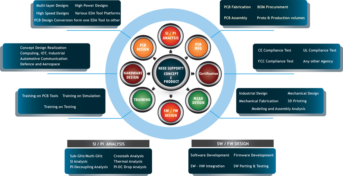
How do I get my Hardware Design realized?
To take up the Hardware Design, the basic input is the block diagram or a reference design with the changes required. The primary aspect would be to describe the end-use application, cost budget for the development, timeline for proto development and the production batches and the unit price for known production batch quantity. With this, the cost of the components, material and production cost will be worked out.
Based on the end-use application, necessary standards the product need to meet has to be reviewed & what government clearances are required to be understood and planned. Further, the same need to be communicated in clear written document for all to follow.
If the design involves Software, Firmware or GUI development, the details of the same need to be described along with the hardware specifications.
Complete PCB design services, incorporating high-layer counts, advanced materials, component miniaturization technologies, and signal integrity.
How to go about the PCB Layout Design for my design?
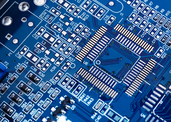
The basic requirement for PCB Design involving component placement and routing the connectivity would be the error-free schematics. The most preferred tool for this in the Electronic Industry would be Orcad, DxDesigner, Pulsonix, Altium Designer, etc.
If you not familiar with any of these tools, the design can be given on paper or in PDF format and the same needs to be entered in any of these tools to proceed for PCB Design.
The PCB Layout Design is done using the EDA Platforms like Cadence Allegro, Mentor Expedition, Mentor PADS, Altium Designer, Pulsonix, etc.
The Choice of the tool depends on the Design Complexity. For simple boards, any of the above tools can be used. But for complex, high-speed boards involving the Signal Integrity / Power Integrity Analyses, the preferred tools are Cadence Allegro and Mentor Expedition / PADS.
All these tools provide the outputs for PCB Fabrication (Gerber File) and for PCB Assembly (BOM and Assembly Drawings).
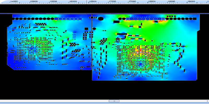
How do I know if my design works properly at high-speeds?
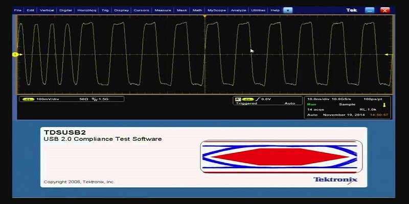
In this situation, the board needs to be subjected to Signal Integrity / Power Integrity Analyses. For this, the basic minimum requirements are the list of critical / high-speed signals on the board, IBIS Models for the devices and operating frequency. While doing the analyses, if any ambiguities are observed, the corrective methods with design changes can be advised for you to approve so that the necessary design changes can be implemented in the design. Further, the analyses is repeated to check if the issue is resolved.
As a final check, you can perform EMI-EMC Analysis on the board to check if it meets the emission standards that are specified by the government agency.
How do I know if the design has any issues relating to driving capacity or optimum number of decaps are used in the design?
Sometimes, the design may have the issues relating to the power supply driving capacity for the design. You can get this analyzed using the Power Integrity DC Drop Analysis.
Use of Decaps is absolutely necessary in the design. But you need to check if an optimum number of decaps are used in the design using the Power Integrity Decaps Analysis. Here, if more decaps are used than that are required, you can save on component cost as well as the required space for accommodating all the components on the board.
.
Where do I get my boards manufactured?
While designing the product, the choice of components and the board form-factor is crucial for saving the board cost.
Total board cost depends on the Board complexity in terms of minimum trace-width & clearance which is driven by usage of fine-pitch BGAs / connectors, Board form-factor versus the total No. of connections on the board, Board finish (HASL, ENIG, OSP), impedance control requirement, etc.
The standard process is to procure the BOM parts in parallel to the PCB Design & Fab process. Hence as soon as the BOM is finalized for the PCB Design, the same needs to be cleared for component procurement. Here, you need to consider the long-lead time parts as well to plan the timely completion of the proto development.
What do I need to provide, to get my system integrated and tested?